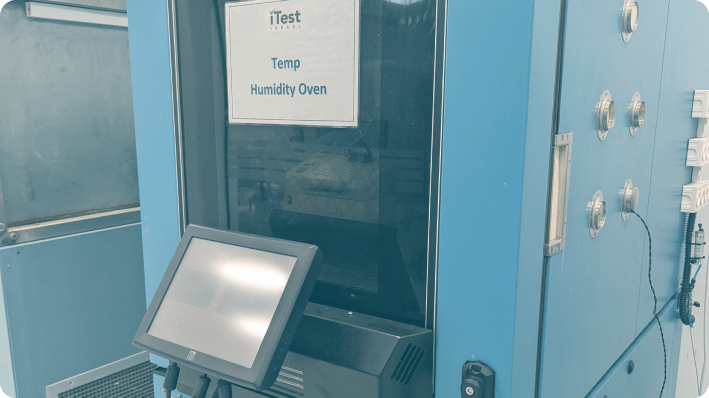
Failure Analysis

We collect and analyze data to determine the cause of failures (either engineering, manufacturing or material). Our combination of engineers, supporting technical staff and equipped laboratories provide OEMs with rapid turnaround time, professional responses, and shorter down time. Through our failure analysis service, OEMs can supply higher quality, more reliable products.
Comprehensive Failure Analysis - From Fault to Fix
- PCB First Article Inspection
- Cross sectioning
- Optical Microscopes with Image Analysis
- Scanning Electron Microscope with EDS
- X-ray Imaging
- C-SAM (Confocal Scanning Acoustic Microscopy)
- Die shear test
- Solder Dip Test
- Wire Bond Pull testers
- Hermeticity Testing
- Die and Pry Testing
- PCB auditing
- IC Plastic Package Decapsulation
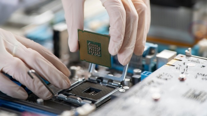
CROSS-SECTIONING
This destructive technique enables the inspection of the construction and/or composition of a section of the components, substrate and solder joints after cutting it apart. When applicable, the sample can be molded in resin to alleviate chipping or destruction of the sample during polishing.

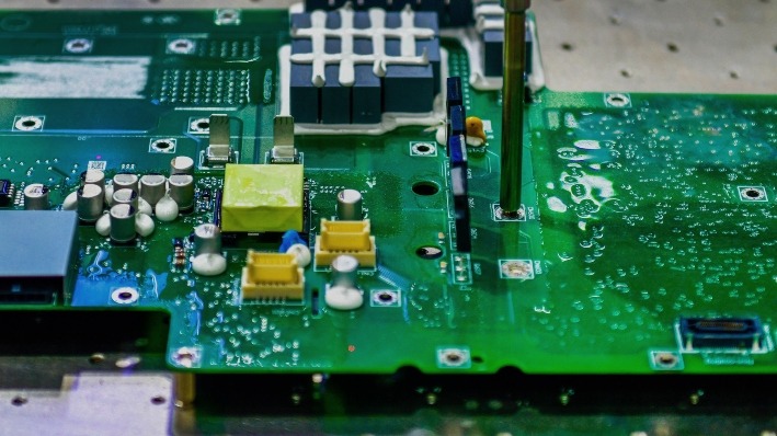
PRINTED CIRCUIT BOARDS
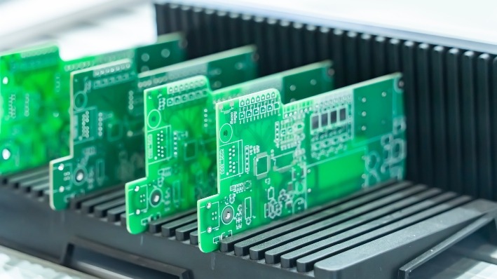
Our customers require a range of test solutions for component loaded Printed Circuit Board Assemblies (PCBA) or bare PCBs (Printed Circuit Boards).
Itest Engineering offers test and inspection strategies including Manual Visual Inspection (MVI), In-Circuit Test (ICT) and Functional Test (FT).
C-SAM
C-SAM (Confocal Scanning Acoustic Microscopy) implements the use of an acoustic microscope to identify delamination, cracks, voids, counterfeit parts, proper bonding of layers and adherence to specification. The product under examination, whether electronic device, printed circuit board or other assembly, is not destroyed in the process. The test results, displayed on an oscilloscope, help the user pinpoint the specific depth of the problematic areas enabling investigation.

DYE AND PRY TEST FOR BGAS
X-Ray Inspection Systems allow 2D or 3D automated or manual inspection of solder joints and other features of electronic devices, PCBs (printed circuit boards) and other electronic components.